Hello,
I'm using my VEMS in an Audi S2 for years now. It is the 3.6 version with oem Audi trigger 135 Wheel and AAN 55 Motronic connector.
I want to use the VW 60-2 hall type trigger wheel and I know I have to solder/desolder some resistors and shortcuts on the board.
After searching hour and hours in www I did not find any information how to do this conversation.
Maybe somebody knows what to modify on the board to use the 60-2? I would appreciate some help.
thx
regards
VEMS modify board from VR to Hall for primary Audi Trigger?
Re: VEMS modify board from VR to Hall for primary Audi Trigg
the wiki is a bit of a minefield of info but this is the page you want:
http://www.vems.hu/wiki/index.php?page=GenBoard%2FManual%2FInputTriggerHardWare
so, reading into it a bit you need to: close SJ2, open SJ6 amongst other things to deal with the primary trigger. the secondary trigger is easy, you just need to disable the auditrigger solder blob which is SJ7 which converts secondary to hall only.
I'll try and give more complete notes later as I have to do this to a customer box this week anyway. I've done it before but stupidly didn't write down notes.
It is highly recommended to bench test your changes with a current limiting power supply on the bench to avoid cooking anything by making a mistake on the board. it also helps to build one of the audio trigger cables via your computers sound card (or a jimstim to simulate a 60-2).
Marc Swanson
Proprietor, EFI Motorsport
Proprietor, EFI Motorsport
Re: VEMS modify board from VR to Hall for primary Audi Trigg
thanks a lot, I will read the wiki and I'm curious about your results...
... I made one mistake in my post above... I have 3.3 not 3.6
... I made one mistake in my post above... I have 3.3 not 3.6
Re: VEMS modify board from VR to Hall for primary Audi Trigg
ok, done and tested. here are my notes:
vr primarty to hall primary:
short sj2 (left of lm1815)
unshort sj6 (below lm1815)
set r30 to 2k7 (2.7k ohm). left of the 2x3 header on top of the board.
2.7k axial resistor from jp6 (2x3 header bottom row, missing hole to the right) to jp1 bottom left pin
5n1 zener from same bottom left pin of jp1 (but usually done on the opposite side so the resistor isn't in the way) to diagonal across pin of jp1 (processor side) stripe facing processor.
regarding the axial resistor, here are pics of that. I cheated and used an existing hall primary ecu as a reference.
use the top and bottom board pdf schematic files for component locations like sj2 and sj6 if you cant find them.
Marc Swanson
Proprietor, EFI Motorsport
Proprietor, EFI Motorsport
Re: VEMS modify board from VR to Hall for primary Audi Trigg
thanks a lot.. is this a 3.3 or 3.6 board?? mine is a 3.3 board...
Re: VEMS modify board from VR to Hall for primary Audi Trigg
3.6. the instructions should be pretty close to the same.
Marc Swanson
Proprietor, EFI Motorsport
Proprietor, EFI Motorsport
Re: VEMS modify board from VR to Hall for primary Audi Trigg
ok, thx... i will have a look in the case soon...
Re: VEMS modify board from VR to Hall for primary Audi Trigg
From reading the schematics I can confirm your steps:
"short sj2 (left of lm1815)
unshort sj6 (below lm1815)
set r30 to 2k7 (2.7k ohm). left of the 2x3 header on top of the board."
but I can not find anything about the two following steps:
"2.7k axial resistor from jp6 (2x3 header bottom row, missing hole to the right) to jp1 bottom left pin
5n1 zener from same bottom left pin of jp1 (but usually done on the opposite side so the resistor isn't in the way) to diagonal across pin of jp1 (processor side) stripe facing processor."
where did you get this information?
And in the wiki, there are additional steps:
"solder JP2 & JP7: this is the top right of the 2x3 header; red on the [image]. The same area of v3.3 looks slightly different (no bottom-right pad, where the blue jumper sits on the image), but never mind. The primary trigger is the same, the changes are at the secondary trigger, eg. 1 throughole pin dropped, and R48 moved to bottom."
for secondary trigger = hall it seems to do nothing because the 3.3 AAN board is already set up for secondary hall??
my English is a little bit poor - I do not really understand the meaning of the following sentence from wiki:
"EC36pin13 is set up for "masking HALL" (nothing to do), but beware, that this setup (with the SJ7 blob shorted) does NOT work for HALL only secondary_trigger ! :"
Re: VEMS modify board from VR to Hall for primary Audi Trigg
black wrote:From reading the schematics I can confirm your steps:
"short sj2 (left of lm1815)
unshort sj6 (below lm1815)
set r30 to 2k7 (2.7k ohm). left of the 2x3 header on top of the board."
but I can not find anything about the two following steps:
"2.7k axial resistor from jp6 (2x3 header bottom row, missing hole to the right) to jp1 bottom left pin
5n1 zener from same bottom left pin of jp1 (but usually done on the opposite side so the resistor isn't in the way) to diagonal across pin of jp1 (processor side) stripe facing processor."
where did you get this information?
from the ecu I took apart that came right from vems configured as hall primary. from a quick look, it appears the function of the 2k7 axial resistor may be similar to soldering jp2 and jp7 in your comment below:
And in the wiki, there are additional steps:
"solder JP2 & JP7: this is the top right of the 2x3 header; red on the [image]. The same area of v3.3 looks slightly different (no bottom-right pad, where the blue jumper sits on the image), but never mind. The primary trigger is the same, the changes are at the secondary trigger, eg. 1 throughole pin dropped, and R48 moved to bottom."
for secondary trigger = hall it seems to do nothing because the 3.3 AAN board is already set up for secondary hall??
yes, but you first have to disable the auditrigger 'bridge'. unshort sj7.
my English is a little bit poor - I do not really understand the meaning of the following sentence from wiki:
"EC36pin13 is set up for "masking HALL" (nothing to do), but beware, that this setup (with the SJ7 blob shorted) does NOT work for HALL only secondary_trigger ! :"
thats the auditrigger I mentioned above. you are bypassing the 'masking' feature and using the hall input only for the secondary.
Marc Swanson
Proprietor, EFI Motorsport
Proprietor, EFI Motorsport
Re: VEMS modify board from VR to Hall for primary Audi Trigg
thanks a lot.. I will have a look in the schematics again...
Re: VEMS modify board from VR to Hall for primary Audi Trigg
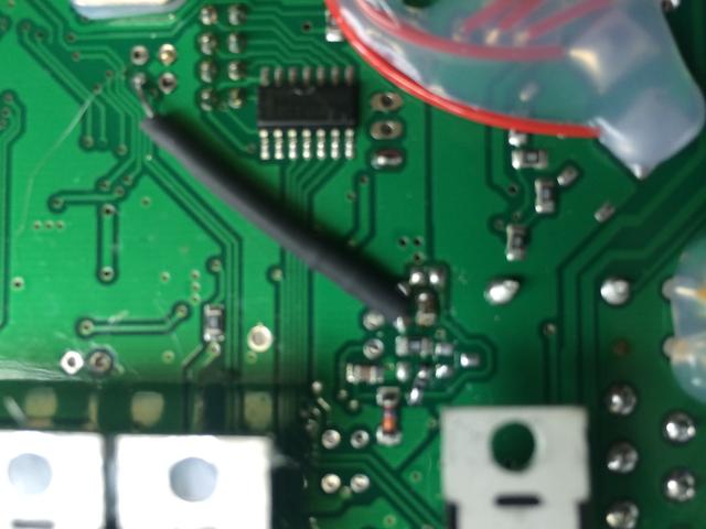
today I opended the case... surprise in VEMStune it is shown as 3.3 but the board has 3.6 sign.
the SJ7 blob is open
there is a bridge like on the first picture (red line): http://www.vems.hu/wiki/index.php?page=GenBoard%2FManual%2FInputTriggerHardWare
SJ7 is open
SJ6 is closed
SJ2 is open
R30 is 183 so 18k
there are no signs of connections like mentioned: "2.7k axial resistor from jp6 (2x3 header bottom row, missing hole to the right) to jp1 bottom left pin
5n1 zener from same bottom left pin of jp1 (but usually done on the opposite side so the resistor isn't in the way) to diagonal across pin of jp1 (processor side) stripe facing processor."
nothing about that...
It seems to be a special conversation. The VEMS case is signed with "HALL HALL AUDI AAN" but the primary trigger seems to be converted from Hall to VR because there a signs of hand soldering at these spots. The former car was running with a 60-2 on the damper.
I think the only thing to do is to change the resistor R30 and close SJ2 and open SJ6... and then it should be Hall Hall again...